UNIVERSITY of PENNSYLVANIA
DEPARTMENT OF ELECTRICAL ENGINEERING
SPICE - A Brief Overview
(URL: http://www.seas.upenn.edu/~jan/spice/spice.overview.html)
This document gives a brief overview of SPICE. The description is far
from complete, as SPICE is a powerful circuit simulator with many capabilities.
However, this document will serve as a start for students in introductory
classes. For more information, please refer to the SPICE user's manual
or books listed at the end of
the document.
Do not print this document on the CETS printers.
-
INTRODUCTION
-
HOW TO SPECIFY CIRCUIT TOPOLOGY AND ANALYSIS?
-
PSPICE - Getting started
-
HSPICE
-
EXAMPLES
-
MODELS of Selected Devices and Components
-
MOST COMMON MISTAKES
-
WHEN SPICE DOES NOT RUN
-
REFERENCES
1. INTRODUCTION
SPICE is a powerful general purpose analog circuit simulator that is used
to verify circuit designs and to predict the circuit behavior. This is
of particular importance for integrated circuits. It was for this
reason that SPICE was originally developed at the Electronics Research
Laboratory of the University of California, Berkeley (1975), as its name
implies:
Simulation Program for Integrated
Circuits Emphasis.
PSpice is a PC version of SPICE (MicroSim Corp.) and HSpice is a version
(Avant!.) that runs on workstations and larger computers. PSpice
is available on the PCs in the SEAS PC computing Labs and HSPICE
is available on ENIAC or PENDER. A complete manual of the Avant!
Star- HSPICE (pdf document) is available as well.
SPICE can do several types of circuit analyses. Here are the
most important ones:
-
Non-linear DC analysis: calculates the DC transfer curve.
-
Non-linear transient analysis: calculates the voltage and current as a
function of time when a large signal is applied.
-
Linear AC Analysis: calculates the output as a function of frequency. A
bode plot is generated.
-
Noise analysis
-
Sensitivity analysis
-
Distortion analysis
-
Fourier analysis: calculates and plots the frequency spectrum.
-
Monte Carlo Analysis
In addition, PSpice has analog and digital libraries of standard components
(such as NAND, NOR, flip-flops, and other digital gates, op amps, etc).
This makes it a useful tool for a wide range of analog and digital applications.
All analyses can be done at different temperatures. The default temperature
is 300K.
The circuit can contain the following components:
-
Independent and dependent voltage and current sources
-
Resistors
-
Capacitors
-
Inductors
-
Mutual inductors
-
Transmission lines
-
Operational amplifiers
-
Switches
-
Diodes
-
Bipolar transistors
-
MOS transistors
-
JFET
-
MESFET
-
Digital gates (PSpice, version 5.4 and up)
2. HOW TO SPECIFY THE CIRCUIT TOPOLOGY AND ANALYSIS?
A SPICE input file, called source file, consists of three parts.
-
Data statements: description of the components and the interconnections.
-
Control statements: tells SPICE what type of analysis to
perform on the circuit.
-
Output statements: specifies what outputs are to be printed
or plotted.
Although these statements may appear in any order, it is recommended that
they be given in the above sequence. Two other statements are required:
the title statement and the end statement.
The title statement is the first line and can contain any information,
while the end statement is always .END. This statement must be a line be
itself, followed by a carriage return! In addition, you can insert comment
statements, which must begin with an asterisk (*) and are ignored
by SPICE.
-
TITLE STATEMENT
-
ELEMENT STATEMENTS
-
.
-
.
-
COMMAND (CONTROL) STATEMENTS
-
OUTPUT STATEMENTS
-
.END <CR>
Format: The statements have a free format and consist of fields
separated by a blank. If one wants to continue a statement to the next
line, one uses a "+" sign (continuation sign) at the beginning of the next
line. Numbers can be integers, or floating points. For example,
RES1 1 0 3500 or RES1 1 0 3.5E3
One can also use the following scale factors:
T(= 1E12 or 10+12); G(= E9); MEG(= E6); K(= E3); M(= E-3);
U(= E-6); N(= E-9); P(= E-12), and F(= E-15)
Both upper and lower case letters are allowed in PSpice and Hspice (SPICE
uses only uppercase characters). As an example, one can specify a capacitor
of 225 picofarad in the following ways:
225P, 225p, 225pF; 225pFarad; 225E-12; 0.225N, etc.
2.1 Data Statements to Specify the Circuit Components and Topology
a. Independent DC Sources
Voltage source: Vname N1 N2 Type Value
Current source: Iname N1 N2 Type Value
-
N1 is the positive terminal node
-
N2 is the negative terminal node
-
Type can be DC, AC or TRAN, depending on the type of analysis (see Control
Statements)
-
Value gives the value of the source
-
The name of a voltage and current source must start with V and I, respectively.
Examples:
Vin 2 0 DC 10
Is 3 4 DC 1.5
The positive current direction through the current or voltage source is
from the positive (N1) node to the negative (N2) node:
Voltage and Current Conventions:
- Spice always assigns a positive reference mark to the 1st node and uses
the passive sign convention to assign the current reference.
- Spice uses the node-voltage analysis. It solves for the unknown node voltages
and also the unknown currents through independent voltage sources.
This gives us a way to find currents flowing in elements: one has to ask for
the current through a voltage source. Thus one can insert an independent voltage
source of zero value in series with the element in which one wants to know
the current, as shown in the example below:
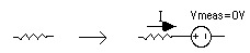
The value of the current will be positive if it flows from the positive to
the negative terminal through the source, as in the above example. Some versions
of PSpice allow you to ask for a current through a resistor without using
a voltage source (EX: I(R1) gives the current in the resistor R1).
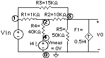
b. Dependent Sources
Voltage controlled voltage source:
Ename N1 N2 NC1 NC2 Value
Voltage controlled current source:
Gname N1 N2 NC1 NC2 Value
Current controlled voltage source:
Hname N1 N2 Vcontrol Value
Current controlled current source:
Fname N1 N2 Vcontrol Value
-
N1 and N2 are the positive and negative terminals of the dependent source,
respectively.
-
NC1 and NC2 are the positive and negative terminals of the controlling
voltage source, respectively.
-
Vcontrol is the zero value voltage source used to measure the controlling
current (the positive current flows into the positive terminal of the controlling
voltage source!).
Examples:
F1 0 3 Vmeas 0.5
Vmeas 4 0 DC 0
c. Resistors
d.Capacitors (C) and Inductors (L)
Cname N1 N2 Value <IC>
Lname N1 N2 Value <IC>
-
N1 is the positive node.
-
N2 is the negative node.
-
IC is the initial condition (DC voltage or current).
-
The symbol < > means that the field is optional. If not specified, it
is assumed to be zero. In case of an inductor, the current flows from N1
to N2.
Example: 
Cap5 3 4 35E-12 5
L12 7 3 6.25E-3 1m
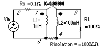
e. Mutual Inductors
A mutual inductance in SPICE is defined by specifying the coupling coefficient
K between the two inductors. The syntax is as follows:
Kname Inductor1 Inductor2 value_of_K
The value of K must be larger than 0 but smaller than 1. Spice does
not support perfect coupling (k=1). The above statement must always be
together with the statements for the two inductors. An example is given
in the figure below. The coupling coefficient K can be calculated as K=M/sqrt(L1xL2)=0.81.
The SPICE statements to define the above coupled coils are as follows.
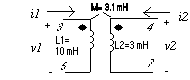
-
L1 3 5 10M
-
L2 4 7 3M
-
K L1 L2 0.81
The DOTS are always associated with the first node of the inductances (i.e.
node no. 3 of L1 and no. 4 of L2). Also SPICE will assign the positive
node voltage to the first node of the inductance (i.e. the DOT) and use
the passive sign convention for the current direction as indicated in the
figure above. For an example circuit see under the section Examples.
f. Ideal Transformer
SPICE has no model for an ideal transformer. An ideal tranformer is simulated
using mutual inductances such that the transformer ratio N1/N2 = sqrt(L1/L2).
Make the coupling factor K close to one (ex. K=0.99999) and choose L such
that wL >> the resistance seen be the inductor. The secondary circuit needs
a DC connection to ground. This can be accomplished by adding a large resistor
to ground or giving the primary and secondary circuits a common node. For
an example circuit see under the section Examples
g. Sinusoidal sources
Vname N1 N2 SIN(VO VA FREQ TD THETA PHASE)
which is a damped sinusoidal voltage source:
Vname = VO + VA exp[-THETA.(t - TD)] sin[2pi.f (t - TD) + (Phase/360)]
-
VO - offset voltage in volt.
-
VA - amplitude in volt.
-
f = FREQ - the frequency in herz.
-
TD - delay in seconds
-
THETA - damping factor per second
-
Phase - phase in degrees
If TD, THETA and PHASE are not specified, it is assumed to be zero.
Example: VG 1 2 SIN(5 10 50 0.2 0.1)
VG2 3 4 SIN(0 10 50)
The last example is an undamped, undelayed sinusoid with an amplitude of
10V and frequency of 50 Hz.
To generate a cosine function, you can make use of the phase relationship
between the sinusoid and cosine. Here is an example of an undelayed cosine
with an amplitude of 5V and frequency of 50 Hz.
Vcos 1 2 SIN(0 5 50 0 0 45)
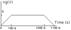
h. Piecewise linear source (PWL)
Vname N1 N2 PWL(T1 V1 T2 V2 T3 V3 ...)
in which (Ti Vi) specifies the value Vi of the source at time Ti
Example:
Vgpwl 1 2 PWL(0 0 10U 5 100U 5 110U 0)
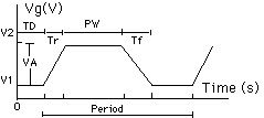
i. Pulse
Vname N1 N2 PULSE(V1 V2 TD Tr Tf PW Period)
V1 - initial voltage; V2 - peak voltage; TD - initial delay time; Tr -
rise time; Tf - fall time; pwf - pulse-wise; and Period - period.
Other sources such as polynominal controlled source, exponential source,
FM-modulated source, etc. can be specified. For information on these components,
check the SPICE manual.
j. Voltage- and Current-controlled Switches
Voltage Controlled:
Current Controlled:
-
N1 and N2 are the terminals of the switch.
-
C1 and C2 are the controlling terminals.
-
Vname is the zero-value voltage source whose current controls the switch.
-
Mname refers to the switch model that is defined in another statement (see
Model Statement below).
The .MODEL statement allows you to specify the parameters of a variety
of devices used in SPICE, such as switches, diodes, transistors. In case
of a switch, we have:
.MODEL Mname Dname(Pvalues)
-
Mname refers to the Mname in the data statement of the switch.
-
Dname is the device name: Vswitch or Iswitch.
-
Pvalues are the values of the switch parameters, such as RON (on - resistance),
ROFF (off-resistance), VON (the control voltage for ON; default = 1V),
VOFF (control voltage for OFF; default = 0V), etc.
Example:
S15 3 5 8 9 SMOD
.MODEL SMOD VSWITCH(RON = 10, VON = 0, ROFF = 100MEG)
k. Operational Amplifiers, and other elements
An operational amplifier can be simulated in different ways. The first
method is to model the amplifier by resistors, capacitors and dependent
sources. As an example an ideal opamp is easily simulated using a voltage
dependent voltage source. The second option uses actual transistors to
model the opamp. The device library contains nonlinear models of the most
common op amps. The student version of PSpice has macromodels for the linear
amplifiers LM324 and uA741 which are included in the EVAL.LIB file. The
professional version comes with library files of many commercial amplifiers
and devices.
An example of the first approach (linear AC model) is given below for
the uA741 opamp. We defined a subcircuit for
the opamp.
SPICE code for the 741 opamp (ref: Macromodeling with Spice,
by J.A. Connelly/P. Choi)
-
* Subcircuit for 741 opamp
-
.subckt opamp741 1 2 3
-
* +in (=1) -in (=2) out (=3)
-
rin 1 2 2meg
-
rout 6 3 75
-
e 4 0 1 2 100k
-
rbw 4 5 0.5meg
-
cbw 5 0 31.85nf
-
eout 6 0 5 0 1
-
.ends opamp741
l. Subcircuits
A subcircuit allows you to define a collection of elements as a subcircuit
(e.g. an operational amplifier) and to insert this description into the
overall circui (as you would do for any other element).
Defining a subcircuit
A subcircuit is defined bu a .SUBCKT control statement, followed
by the circuit description as follows:
-
.SUBCKT SUBNAME N1 N2 N3 ...
-
Element statements
-
.
-
.
-
.
-
.ENDS SUBNAME
in which SUBNAME is the subcircuit name and N1, N2, N3 are the external
nodes of the subcircuit. The external nodes cannot be 0. The node numbers
used inside the subcircuit are stricktly local, except for node 0 which
is always global. For an example, see Operational Amplifier above.
Using a subcircuit
The element statement for a subcircuit is similar to any other
element. The format is as follows:
Xname N1 N2 N3 ... SUBNAME
in which Xname refers to the element (subcircuit) being used; N1, N2, N3
are the nodes to which the external nodes of the subcircuit are being connected,
and SUBNAME is the name of the subcircuit being used.
An example of an inverting opamp circuit using the subcircuit
of the the uA741 (see operational
amplifiers above) is given below. The subcircuit is called x1.
-
vs 1 0 dc 5
-
r1 1 2 200
-
rf 2 3 1k
-
x1 0 2 3 opamp741
-
.dc vs 0 10 1
-
.plot dc v(3)
-
.end
m. Semiconductor Devices
Most of the elements that have been described above require only a few
parameters to specify its electrical characteristics. However, the models
for semiconductor devices require many parameter values. A set of device
model parameters is defined in a separate .MODEL statement and assigned
a unique name. This method alliaviates the need to specify all of the model
parameters on each device element card. Thus a semiconductor device is
specified by two command lines: an element and model statement.
The syntax for the model statement is:
.MODEL MODName Type (parameter values)
MODName is the name of the model for the device. The Type refers to the
type of device and can be any of the following:
-
D: Diode
-
NPN: npn bipolar transistor
-
PNP: pnp bipolar transistor
-
NMOS: nmos transistor
-
PMOS: pmos transistor
-
NJF: N-channel JFET model
-
PJF: P-channel JFET model
The parameter values specify the device characteristics as explained below.
m1. Diode
Element line: Dname N+ N- MODName
Model statement:
.MODEL MODName D (IS= N= Rs= CJO= Tt= BV= IBV=)
The element name starts with D to indicate that the element is a diode,
N+ and N- are the two node numbers and MODName is the name of the model
of the diode which is specified in the model line. The values one can specify
include: the saturation current, IS (default=1E-14A), the emission coefficient,
N (=1), the series resistance, RS (=0 ohm), junction capacitance, CJO (=0F),
transit time, TT (=0sec), reverse bias breakdown voltage, BV (=infinite)
and the reverse bias breakdown current, IBV (=1xE-10A). If a parameter
is not specified the default value (given in parenthesis) is assumed.
As an example, the model parameters for a 1N4148 commercial diode
are as follows:
.model D1N4148 D (IS=0.1PA, RS=16 CJO=2PF TT=12N BV=100 IBV=0.1PA)
m2. Bipolar transistors
Element: Qname C B E BJT_modelName
Model statement:
.MODEL BJT_modName NPN (BF=val IS=val VAF=val)
in which BF is the common emitter current gain ß, IS is the saturation
current and VAF is the Early voltage. If no values are specified, the default
values are assumed (ß=100; IS=1E-16A, and VAF=[infinite]). Other
parameters can be specified including the junction capacitances CJE (0pF)
and CJC (0pF), the transit times TT (0sec) and TR (0sec), the base RB (0
Ohm), emitter RE (0 Ohm) and collector resistances RC (0 Ohm). For a complete
list of the parameters please refer to one of the references. As an example,
the model parameters for the 2N2222A NPN transistor is given below:
.model Q2N2222A NPN (IS=14.34F XTI=3 EG=1.11 VAF= 74.03 BF=255.9
NE=1.307 ISE=14.34F IKF=.2847 XTB=1.5 BR=6.092 NC=2 ISC=0 IKR=0 RC=1 CJC=7.306P
MJC=.3416 VJC=.75 FC=.5 CJE=22.01P MJE=.377 VJE=.75 TR=46.91N TF=411.1P
ITF=.6 VTF=1.7 XTF=3 RB=10)
Notice that the continuation sign + should be added at the beginning of
a new line. A circuit example with a npn transistor can be found under
the section Examples
m3. MOSFETS
Element: Mname ND NG NS <NB> ModName L= W=
The MOS transistor name (Mname) has to start with a M; ND, NG, NS and
NB are the node numbers of the Drain, Gate, Source and Bulk terminals,
respectively. ModName is the name of the transistor model (see further).
L and W is the length and width of the gate (in m).
The above paramters are usually sufficient when specifying discrete
transistors. However, for integrated circuit simulations one need to specify
several other parameter values related to the transistor geomtry. These
are optional.
Mname ND NG NS NB ModName <L=VAL> <W=VAL> <AD=VAL>
<AS=VAL> <PD=VAL> <PS=VAL> <NRD=VAL> <OFF>
<IC=VDS.VGS.VBS>
in which
AD and AS are the area of source and drain diffusion (in sq. m).
PD and PS are the value (in m) of the perimeter of the source and drain.
NRD is the number of squares of the drain diffusion for resistance
calculations.
OFF sets the starting condition to OFF.
The initial condition specification using IC=VDS, VGS, VBS is intended
for use with the UIC option on the .TRAN card, when a transient analysis
is desired starting from other than the quiescent operating point. See
the .IC card for a better and more convenient way to specify transient
initial conditions.
Model statement:
.MODEL ModName NMOS (KP= VT0= lambda= gamma=)
in which KP=uCox and VTO is the threshold voltage. The default values are
KP=20uA/V2; and the rest is equal to 0. There are several other
transistor parameters that can be specified, in particular when doing simulations
of integrated circuits. The general form of the .MODEL statement is as
follows:
LEVEL refers to the MOSFET model that describes the terminal I-V characteristics
of the transistors. LEVEL 1 is the simplest Mosfet model and is in general
sufficient for describing discrete transistors as is done in the EE216
and EE319 courses. However to simulate integrated circuit transistors,
one need to use a more sophisticated models. LEVEL 2 includes extensive
second-order models, while LEVEL 3 is a semi-empirical model that is better
suited for short-channel transistors. Another model that is especially
suited to model short-channel effects is called the BSIM model (LEVEL 13
in HSpice).
For partial listing of the MOSFET
MODEL parameters click here. Refer to the references for a complete
list of parameters.
An example of the model parameters of the 1.2um
CMOS MOSIS transistors can be found in section on Models of Selected
Devices and Components later on.
m4. JFETS
Element: Jname ND NG NS ModName
ND, NG, and NS are the node numbers of the Drain, Gate, and Source terminals,
respectively. ModName is the name of the transistor model
Model statement:
for the N-JFET and P-JFET respectively. A partial list of the parameters
that can be specified is: VT0 (threshold voltage, -2V default for N_JFET),
BETA (transconductance coefficient, 1E-4 A/V2), LAMBDA (channel length
modulation, 0 /V), IS (gate p-n saturation current, 1E-14A), CGD and CGS
(drain and source zero-bias junction capacitances, 0pf), RD and RS (drain
and source ohmic resistances, 0 Ohm).
For an example of the model parameters of the
2N5459 N-JFET see section on Models of Selected Devices and Components
later on.
2.2 Commands or Control Statements to Specify
the Type of Analysis
a. .OP Statement
This statement instructs Spice to compute the DC operating points:
-
voltage at the nodes
-
current in each voltage source
-
operating point for each element
In PSpice it is usually not necessary to specify .OP as it gives you automatically
the DC node voltages. However, HSpice does not give the DC voltages unless
you have specified a certain analysis type, such as for instance .TRAN,
or .AC analysis (Spice automatically does a DC analysis before doing a
transient or AC analysis). Thus, if you are only interested in the DC voltages
in HSpice, you should specify the .OP option, or the .DC option (see further).
b. .DC Statement
This statement allows you to increment (sweep) an independent source over
a certain range with a specified step. The format is as follows:
.DC SRCname START STOP STEP
in which SRC name is the name of the source you want to vary; START and
STOP are the starting and ending value, respectively; and STEP is the size
of the increment.
When the Start and Stop values are identical (and the Step is non-zero),
the .DC command produces only one value. This may be usefull in HSpice
when you do not want all the DC voltages and currents to be printed (with
the .OP option), but are interested in a limited number of DC voltages
and currents. In the .PRINT statement (see further)
you would then also specify the node voltages you like to know (ex. .DC
Vs 3 3 1 and .PRINT DC V(2), V(3), I(Vmeas) ).
You can nest the DC sweep command which is often used to plot transistor
characteristics, such as the Drain current ids versus the Drain-source
voltage Vds for different gate voltages Vgs. This can be done as follows:
In the example above, the voltage Vds will be swept from 0 to 5V in steps
of 1V for every value of Vgs.
c. .TF Statement
The .TF statement instructs PSpice to calculate the following small
signal characteristics:
-
the ratio of output variable to input variable (gain or tranfer gain)
-
the resistance with respect to the input source
-
the resistance with respect to the output terminals
in which OUTVAR is the name of the output variable and INSRC is the input
source.
The .TF statement can be used to find the Thevenin small signal equivalent
resistance. (The Thevenin voltage is given by the node voltage at the
open circuit terminal, as a result of the .OP statement). See also Output
Statements later on.
d. .SENS Statement
This instructs PSpice to calculate the DC small-signal sensitivities of
each specified output variable with respect to every circuit parameter.
.SENS VARIABLE
Example: .SENS V(3,0)
e. .TRAN Statement
This statement specifies the time interval over which the transient analysis
takes place, and the time increments. The format is as follows:
.TRAN TSTEP TSTOP <TSTART <TMAX>> <UIC>
-
TSTEP is the printing increment.
-
TSTOP is the final time
-
TSTART is the starting time (if omitted, TSTART is assumed to be zero)
-
TMAX is the maximum step size.
-
UIC stands for Use Initial Condition and instructs PSpice not to do the
quiescent operating point before beginning the transient analysis. If UIC
is specified, PSpice will use the initial conditions specified in the element
statements (see data statement) IC = value.
See also Output Statements later on.
f. .IC Statement
This statement provides an alternative way to specify initial conditions
of nodes (and thus over capacitors).
.IC Vnode1 = value Vnode2 = value etc.
g. .AC Statement
This statement is used to specify the frequency (AC) analysis. The format
is as follows:
-
.AC LIN NP FSTART FSTOP
-
.AC DEC ND FSTART FSTOP
-
.AC OCT NO FSTART FSTOP
in which LIN stands for a linear frequency variation, DEC and OCT for a
decade and octave variation respectively. NP stands for the number of points
and ND and NO for the number of frequency points per decade and octave.
FSTART and FSTOP are the start and stopping frequencies in Herz
Example: .AC DEC 10 1000 1E6
See also Output Statements later on. For an example
circuit see under the section Examples.
h. For .NOISE, .DISTO, and .FOUR statements
Please consult the manual.
2.3 Output Statements
These statements will instruct PSpice what output to generate. If you do
not specify an output statement, PSpice will always calculate the DC operating
points. The two types of outputs are the prints and plots. A print is a
table of data points and a plot is a graphical representation. The format
is as follows:
in which TYPE specifies the type of analysis to be printed or plotted and
can be:
The output variables are OV1, OV2 and can be voltage or currents in voltage
sources. Node voltages and device currents can be specified as magnitude
(M), phase (P), real (R) or imaginary (I) parts by adding the suffix to
V or I as follows:
-
M: Magnitude
-
DB: Magnitude in dB (deciBells)
-
P: Phase
-
R: Real part
-
I: Imaginary part
Examples:
.PLOT DC V(1,2) V(3) I(Vmeas)
.PRINT TRAN V(3,1) I(Vmeas)
.PLOT AC VM(3,0) VDB(4,2) VM(2,1) VP(3,1) IR(V2)
This page has been  accessed since
Jan. 12, 1996.
accessed since
Jan. 12, 1996.
Back to Table of Contents
Jan Van der Spiegel
jan@ee.upenn.edu
Created Sept. 30, 1995; Updated October 15, 1995